Printed circuit boards which may also be called Printed wiring boards or Printed wiring cards are the fundamental blocks in advanced modern circuits and advanced modern electronics. The evolution and serendipity of manufacturing and designing technology has pushed the complexity and complications of the electric integrated circuits to new horizons. For example the integrated quantum circuits and Intel core i7 processor contains of transistors on a single circuitry. Before the dawn of PCB designing the circuits were built through the arduous practice of point to point wiring which was expansive, time consuming and limited in its capacity and efficiency. The problems associated with conventional circuits were also numerous ranging from frequent failures at connections, short circuits, loss of insulation, overheating, wear and tear and short life span of the circuits.
This led to the invention of modern techniques i.e. silicon and integrated circuits technology. The cost of electrons drastically decreased while the efficiency of these circuits vehemently increased. The integrated circuits greatly helped reduce the size of the circuitry and hence a new era of modern inventions in electronics began to take shape. According to Moore’s law the number of transistors which can be fit in dense integrated circuits double every year.
A printed circuit board in its essence is a board or a card which provides ways and means i.e. physical and electrical of connecting the electronic components. A PCB is a rigid board made from laminate comprising of mostly glass epoxy base material with coating of copper on single or either side of it. The rigid board provides physical means for handling or mounting the electronic components of an integrated circuit on it while the copper coating allows the drawing of copper paths which acts as wires for the conduction of electricity between the components.
The tracks of copper wires leading electric current to various components are etched according to the software design of the integrated circuits. By the use of PCB designing software’s i.e. Altium, Proteus or PCB CAD, the PCB layout of the circuit is prepared which is printed on the actual PCB board. The PCB is treated with special chemicals so that the tracks of the wiring are left behind while the excess copper is dissolved. The printed circuit board without any electronic component on it while only containing the tracks is aptly called the Printed wrings board or PWB.
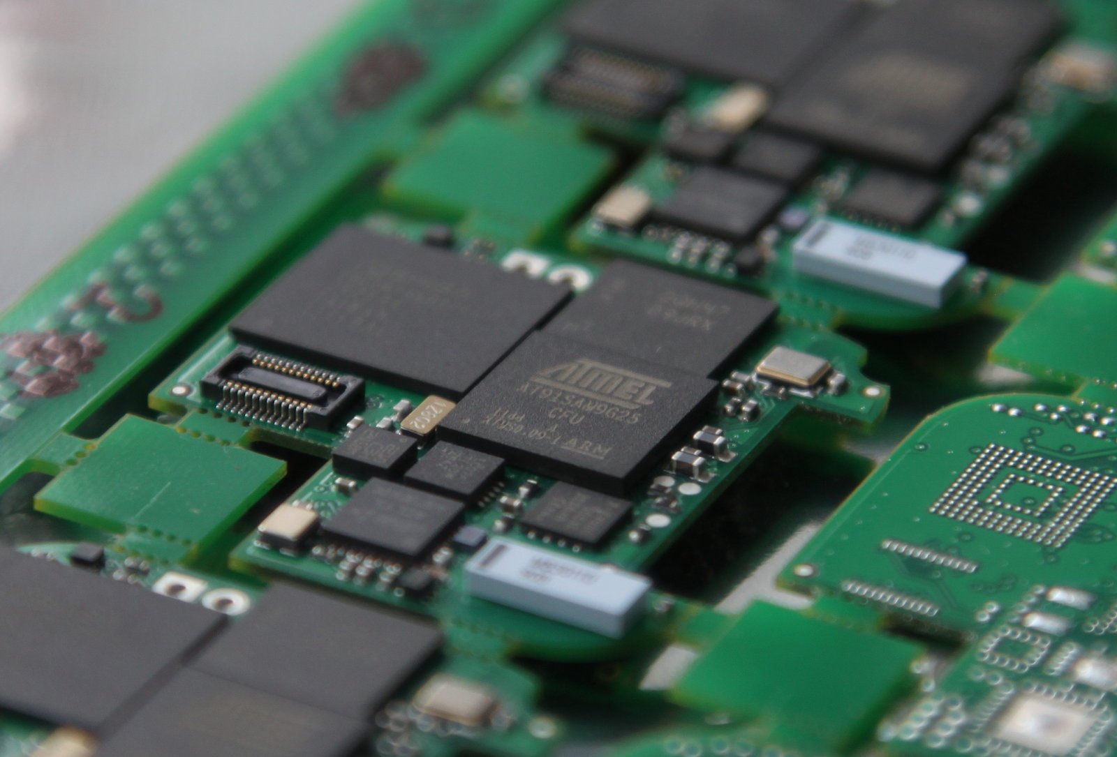
The Printed circuit board Assembly or PCBA is the process of mounting electronic components on the Printed circuit boards. The components are mounted and assembled as per their designated position on the board as per the design of the integrated circuit. The components are affixed on the designated position through soldering which is the fundamental part of the printed circuit board assembly PCBA process.
In the printed circuit board designing, three types of boards are used i.e. single sides boards, double or dual sided boards and multi-sided printed circuit boards. The single sided boards only contain copper layer on one side of the laminated material while in the dual sided board, there is conducting layer on both sides of the board. The copper layer in double circuit board on two sides can be of varying thickness depending upon the requirement of the application it is supposed to be employed in. The single circuit boards are mostly used in low density designs while double and multi-sided designs are mainly used in high density designs.
The single sided PCBs dominate the market in terms of sheer volume as they are least expensive and provide a quick and cost effective solution to most problems in electronic circuits. Single sided PCBs have low probability of manufacturing issues. They are popular, common and are most familiar with most PCB manufacturers. Though theses PCBs are usually simple but still they are also reemployed in highly significant and complex electronic devices i.e. Power supplies, Relays, Radio, surveillance etc.
Double sided PCBs have conducting layer of copper on both sides of the rigid lamination and hence allow for higher density designs. The two sides of the PCB come into play in the integration of the electronic circuits. The printing on the two sides in just as in case of the single sided PCB but in this case the two layers aren’t separate but the two layers of the same circuit. The two sides interact with each other communicating singles and voltage from one side and another through vias. However the main difficulty in the dual sided PCBs is the alignment of the holes as they should be in the aligned positions on both sides of the board. The offset in alignment can lead to severe design and operational complications as the offset should not anything more than one fifth of an inch. The inspection of the double sided PCB through various stages is of utmost importance as it will allow the repair of design mistakes instantly.
The double sided PCBs are more flexible for the designers as they allow greater circuit density. The double sided PCBs can help reduce the cost of the integrated circuit as well by allowing more components in relatively small size. Double sided PCBs are mostly used in industrial controls, control relays, HVAC systems, hard drives, printers, amplifiers, test equipments etc.
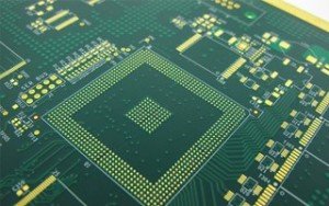
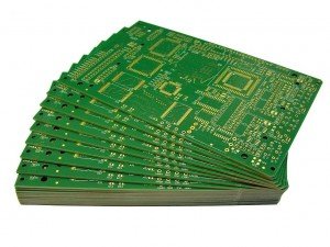
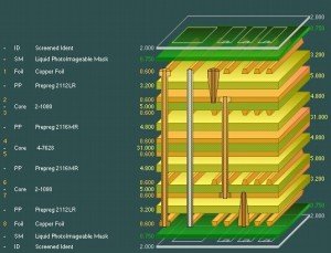
The third type of PCBs is the multi-layer PCBs which contain more than two layers. Multiple layers are made from the same base material which can range from basic epoxy glass to exotic ceramic or Teflon material but with copper coating on top, bottom and one or more inner layer cores. The number of cores corresponds with the number of layers in the multi-layer PCBs. The thickness of the core for various layers can typically vary from 0.038” to 0.005”. Multi-layer PCBs provide higher assembly density, smaller size, increased flexibility and easier incorporation. The Multi layer PCBs are mainly used in computers, file servers, data storages, GPS technology, X rays equipment, cell phone transmission and internal circuitry and enumerate number of other such complex integrated circuits.
The concept of advanced modern circuitry hence is complete without the mention of high tech PCBs. There is a need now more than ever to invest in the design and manufacturing of efficient and cost effective PCBs. SynergizePCB is such an initiative to meet your extraordinary demands with care, quality control and cost effective solutions.