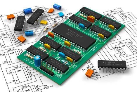
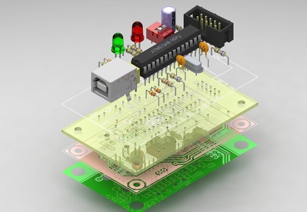
The computer aided printed circuit board design is the fundamental basis for the PCB manufacturing and assembly as it effects the operation, layout and the smooth working of the printed circuit board. The software aided design makes up the doctrine of the PCB so the drawing of the circuitry in PCB software deserves standard practices of design and quality inspection checks to be performed. For the designing of the printed circuit boards, two files from the PCB software i.e. Gerber Files and drill or Excellon files are required.
The process of obtaining theses files involves the drawing of the integrated circuit through the use of software which can give the Gerber Files i.e. the files outlining the copper foil tracks on the PCB and the Drill Files or Excellon files i.e. files which give details of drilling pattern on the Printed Circuit Boards (PCBs).
The software designing is mostly done on PCB software like Altium, Proteus and CAD which give comprehensive computer aided designs. The Gerber files and drill files can be printed and iron on the surface of the Printed Circuit Boards (PCBs) or in a completely automated environment, they can be made use of by the designing machines where the patterns of the Gerber and drill files are etched on the surface of the Printed Circuit Boards (PCBs). The etching of the copper tracks on the PCB is done as per the software provided diagrams.
There are a lot of recommended design checks during process of working on the PCB software for obtaining the Gerber and the drill files. We will discuss some of the most common and standard design checks which are performed in the process of printed circuit board design at SynergisePCB Inc.
1) In multi-layer Printed circuit boards, there are via for the conduction of voltages between the layers and SMT pads for the mounting of the components on the PCB. Most of the time due to less space on the printed circuit board, the designers tend to place the via and the SMT pad very close to each other. This can lead to short circuiting between the components of the printed circuit board and design faults. This is why it needs special care to make sure via and the SMT pads are not too close to each other and there is reasonable gap between them.
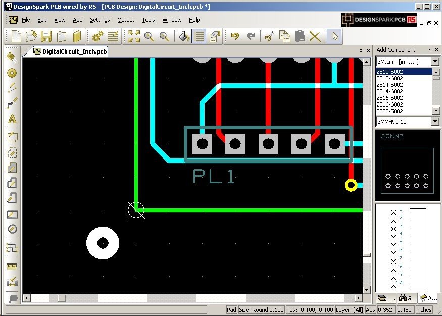
2) The traces in the PCB should be in a uniform manner instead of complex and illogical structure. It is standard practice to keep the traces at least 90 degree or greater angle. In such cases when acute angles are kept between the traces, the design failures arise at later stages.
3) For the SMT pads, it should be given significance that they are not too close to the PCB outline. There should always be reasonable distance between the outline and the pads where the components are to be mounted. In case the pads are too close to the outline, it can lead to physical and operational faults in the printed circuit boards.
4) The sizing of the Holes in the printed circuit board design is one of the most important design parameter to be taken care of. The sizes of the holes should be appropriate as per the components to be fit inside of them. Different components come in various sizes and connecting wires so it is highly standard practice to take their measurements in consideration before finalizing the size of the holes.
5) In multilayer printed circuit boards, enough clearance should be left between the plated through holes and other copper features on the other layers which are not supported by the plated through hole. The minimum standard clearance to be left is 0.006” while more space should be left where possible.
At SynergisePCB Inc. we give extreme importance to design checks of various kinds in the initial and development stages of the PCB designing so no fault or unforeseen circumstances have to be dealt with at the later stages. It wouldn’t be an overstatement to say that we care about the design efficiency and reliability of our products more than any other competitor in this business and we have a proven track record of delivering excellent services.