PCBs can be classified into various denominations depending on the basic criterion behind the classification but the most common criteria for the classification is the number of layers contained the PCB. PCBs with reference to their layers can be classified into their main categories i.e. Single sided Printed circuit boards, Double/Dual sided Printed circuit boards and Multi sided or Multi layered printed circuit boards.
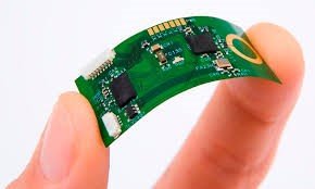
1) Single Sided Printed Circuit boards]
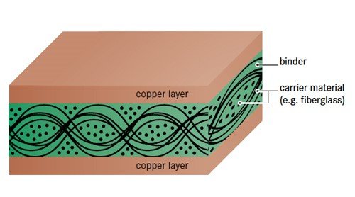
The single sided printed circuit board consists of rigid lamination of either glass epoxy resins or ceramic material while the copper layer is coated only on one side of the PCB. The thickness of the copper layer can vary depending upon the application. A protecting mask of solder can be applied on the top of copper layer. In a single sided PCB all the components in the PCBA are assembled on one side only.
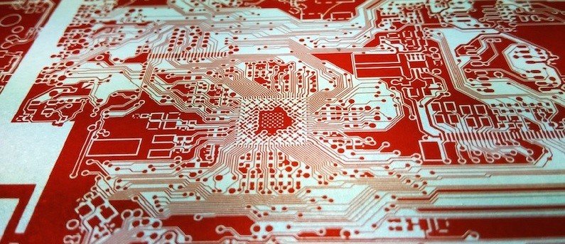
Hence the single sided PCBs are used in low density applications where a lot of components are not being connected. The advantage of the single sided PCBs is that they tend to cost less; they are easy to manufacture and work with as most manufacturers are familiar with them. Their main disadvantage of the singe sided PCBs is that they cannot be used in high density applications where greater number of components is to be connected in the integrated circuit as if single sided PCB were to be used in this case, it would tend to increase the cost.

Some of the major applications in which PCBs are to be used are as follows,
- Power Supplies
- Light emitting diode circuitry
- Arithmetic Calculators
- Timing circuits i.e. clocks
- Relaying circuits
2) Double sided Printed Circuit boards
The double sided Printed Circuit boards consist of the same rigid laminated material for providing physical support to the electronic components while the conduction of electricity, there is copper layer on both sides of the substrate. The two sides of the double sided PCBs are used for integrated the same circuit. The printing on the two sides in just as in case of the single sided PCB but in this case the two layers aren’t separate but the two layers of the same circuit. The two sides interact with each other communicating singles and voltage from one side and another through vias.
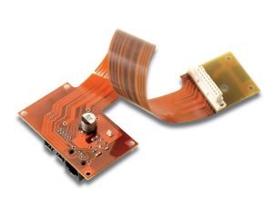
However the main difficulty in the dual PCBs is the alignment of the holes as they should be in the aligned positions on both sides of the board. The offset in alignment can lead to severe design and operational complications as the offset should not anything more than one fifth of an inch. The inspection of the double sided PCB through various stages is of utmost importance as it will allow the repair of design mistakes instantly.
The two sides of the PCB in case of double sided PCB is connected through via. The via in PCB are the means of provided the connection for transmission of single and voltage between the two layers of the PCBs. Via is a hole of miniature size which can replicate the voltages on one side on the other side of the PCBs as required.
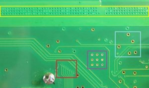
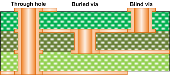
Via most commonly employed in double sided PCB is the plated through via or via in pad while in multi layer PCBs the other type of via i.e. buried via and blind via also play their part as per required. Via on one hand provide greater flexibility to the designing and efficiency of the circuitry but at the same time it also complicates the manufacturing of the PCB. Greater care is required in connecting the two sides as little offset in drilling via can lead to severe complications in the operation of the PCB.
The major advantage of the double sided PCB is the greater circuit density capability available with double sided PCBs. It also has intermediate level of complexity for high level applications and reduced cost and size of the integrated circuit.
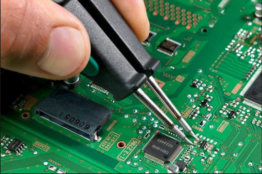
Some of the common devices which employ double sided PCBs for their operations are as follow,
- Data Storage Devices
- Industrial Relays
- Communication Systems
- HVAC systems
- UPS Systems
- Test equipments
- Traffic light Systems
3) Multi layer Printed Circuit Board
The third type of Printed circuit boards is the Multi layer printed circuit board which contains more than two layers. . Multiple layers are made from the same base material which can range from basic epoxy glass to exotic ceramic or Teflon material but with copper coating on top, bottom and one or more inner layer cores. The number of cores corresponds with the number of layers in the multi-layer PCBs. The thickness of the core for various layers can typically vary from 0.038” to 0.005”.
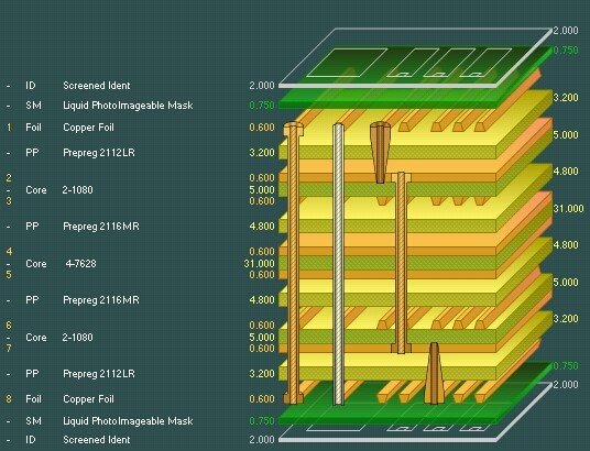
Multi layer PCBs are made by laminating alternating and layers of the substrate material and the prepeg together at high temperature and pressure such that no air bubble is trapped between them. Prepeg and core are effectively the same material but the prepeg is not cured which distinguishes it from the core.
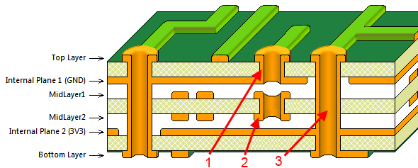
The different layers of the multi layer PCB are also connected through via. Via used in Multi layer PCB are of three different kinds i.e. Plated through via, buried via and the blind via. The plated through via connects the top most and bottom layer of the multi layer PCB. The Buried via connects two of more layers of via in the core of the multi layer PCB but doesn’t connect the top and the bottom layer. The blind via is the type of via which connects the two or more layers but it cannot be seen through it. There are also micro via which are used when very small connections at micro levels are to be made. The connections through via are greatly increases the complexity of the PCB as they are extremely sophisticated to deal with.
Some of the devices which use Multi Layer PCBs are as follows,
- Computers
- GPS systems
- Nuclear Detection Systems
- Space exploration mission’s circuitry
- Specialized medical equipment technology
Synergize PCB Inc. provides facility of PCB manufacturing up to 70L with greatest quality in manufacturing, cost effectiveness and high reliability of premium quality products.
