At SynergisePCB Inc. the flexible PCB manufacturing and designing have a smooth flow of standard practices which can be easily described in the manner of various stages, with each step categorically describing the particular practice followed in the development process. The Manufacturing of the Flexible Printed Circuit Boards (FPCBs) involves the selection of material i.e. laminate and copper foil. Some of the most common materials used in the manufacturing of the Flexible Printed Circuit Boards (FPCBs) are paper reinforced phenol, paper reinforced epoxy and woven glass reinforced epoxy and Teflon material. Some of the properties which are commonly kept in consideration for the selection of material for the manufacturing of Flexible Printed Circuit Boards (FPCBs) are greater cutting and drilling properties. The ability of a material to withstand the application of chemical and acids is also given precedence during the material selection.
The second stage in the manufacturing of flexible printed circuit board is the selection and application of the conducting material on the top of the substrate. Copper is the standard and highly common material used for circuit traces and provides the best and cost effective solution. Thickness of the copper layer for the flexible printed circuit boards can typically ranges from .0007″ to .0028″. At SynergisePCB Inc. we can work with both kinds of adhesive based and adhesive less substrate or base materials. SynergisePCB Inc. also has the capability to manufacture circuits having the metal core as commonly known as Metal core Printed circuit boards for rigid flex printed circuit boards in order to provide more support for specific applications. Some examples are stainless steel for corrosion resistance, BeCu for spring properties, Cupronickel for high resistance applications.
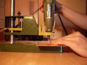
 The next stage of the PCB development is the drilling of holes as per the drilling file obtained from the computer-aided design software. The drilling tools used are made of tungsten-carbide ranging in size from few micrometres to few millimetres. The size of the holes or via depends upon their type and application in the Printed Circuit Boards (PCBs).

Plated through holes are commonly employed in the flexible printed circuit boards for the communication of signals between various layers of the PCB. Plated through via connects the top and the bottom layer of the multi layer Printed Circuit Boards (PCB). In order to spot a plated through hole, you can see if the light passes through it or it is possible to see through it. Plated through holes are the simplest kind of holes and they only need drilling or laser light to be drawn. Drilling of plated through holes is relatively cheap but they may take up more space as compared with the other types of via or the micro via.

Insulation is provided to the substrate of the multilayer Printed circuit board in order to prevent the communication of unwanted signals through via or surface of the substrate between different layers of the printed circuit board. The insulation layer provided is the prevention layer or cover layer placed over the conducting area which is left exposed. The insulation or cover layer is generally constructed of a layer of the polyimide film laminated or pressed over the copper layer the adhesive techniques or through the use of high technology machinery.

For high density applications, SynergisePCB Inc. can provide the ability to work with Photo Imaging or AOI standard insulation layer. The material is thus coated over the copper layer and does not require adhesive or lamination. Photo imaging insulation layer can be provided with either various colors pigments as well for better handling of the equipment.

The Printed Circuit Board or the printed wiring board becomes a Printed Circuit Boards Assembly (PCBA) when the electronic components are placed on it on their designated places. The assembling process involves drilling of holes and via onto the Printed Circuit Boards for connections and placements of the components on the PCB, application of soldering paste, the application of surface mount technology for careful placing of the components on their designated paces, Reflow soldering for solidifying the connections made between the components and the soldering paste. Once the connections have been made, the inspection and quality assurance tests are performed to trace and fix any fault in the assembly. Once the assembly is complete and quality assurance tests have been performed the Printed Circuit Boards assembly is than sent for final inspection and functional testing to analyze its testing under normal conditions under which it is supposed to work. If it gives positive results the product is then sent for the commercial use.
At SynergisePCB Inc. we can take care of your wide range of design, shape, quality and efficiency requirements for the flexible printed circuit boards through our vast experience in this field of work and meeting the requirements and satisfaction of our wide range of clients all over the world. The instruments and technical ability at our hand can exceed the capability of any other firm in this field anywhere in the world. Our products are specialized with all manufacturing managed in the United States of America under the strict and standardized methods of quality control, management, operation and customer support.

