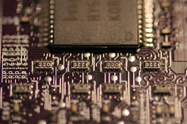
There are different ways of carrying out copper patterning during the manufacturing of printed circuit board products and creating effective patterns, which are capable of supporting high definition applications in standard devices. Similarly, the copper patterning has to be carried out on different scales depending upon the nature of the printed circuit boards and the devices for which they have to be manufactured. These requirements are usually divided as large volume copper patterning, small volume copper patterning, and hobbyist. The techniques of carrying out patterning on all these different scales are different and in this article, we will discuss the techniques that are usually employed for carrying out catering for a large volume.

There are two techniques that are popular for carrying out copper partnering at large volume and include Silkscreen printing and photoengraving. The techniques are also used depending upon the advantage that they provide under different circumstances and are used commonly in industry. An explanation of the two techniques is given below:
- Silkscreen printing: This type of printing is used for PCBs, which have large features and where printing patterning is required on large volume manufacturing. This technique is popular for properly managing printing of printed circuit boards with bigger features and providing high-quality results.
- Photoengraving: It is a highly popular technique that is used when more final features are required which are not usually provided by Silkscreen printing. The precision and accuracy of photoengraving are much higher as compared to Silkscreen printing, however, it has also costly as compared to the other technique.
SynergisePCB is one of the leading manufacturers of Printed Circuit Board products all over the world and we offer our products to clients manufactured through high-quality methods and techniques. Please feel free to contact us your contact form or contact number available on our website.
