
In the world of electronics, reliability of the electronic circuits is a precious attribute. The user expects the devices to perform perfectly without interruption and expect long term operation of the device. Ensuring high quality operation requires robust and unfailing protection from intense and drastic conditions.

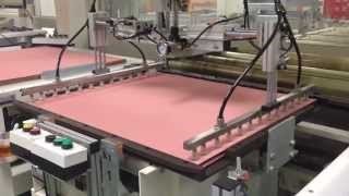
The fundamental protection to be provided to the printed circuit board is the lamination provided to the board. A printed circuit board in its essence is a board or a card which provides ways and means i.e. physical and electrical of connecting the electronic components.
A PCB is a rigid board made from laminate comprising of mostly glass epoxy base material with coating of copper on single or either side of it. The rigid board provides physical means for handling or mounting the electronic components of an integrated circuit on it while the copper coating allows the drawing of copper paths which acts as wires for the conduction of electricity between the components. In order to ensure that the conducting paths don’t pass singles, lamination in the form of substrate is provided to the printed circuit board. The lamination requirements of various kinds of printed circuit boards depend upon their nature, type and the area of use.
We will look into the lamination requirements of various types of printed circuit boards in detail:-
Lamination of Multi-layer Printed Circuit Board

Multi layer Printed Circuit Boards (PCB) are like single or double layer Printed Circuit Boards (PCB) but in multi layer Printed Circuit Boards (PCB), the layers are substrate and copper coating exceed from two layers. The layers of the multi layer printed circuit board can be either trace layers or etched boards. The layers of the multi layer PCB are connected or bonded together with the help of the lamination. The internal layer of the multi layer PCB is subjected to high temperature and pressure. The high temperature and pressure is then slowly released so the laminated material applied cools down and solidifies.
Multi layer Printed Circuit Boards (PCB) has greatest and complex functional capability of all types of PCBs available today as they are used in wide range of consumer electronics i.e. smart phones and microwaves.

Lamination of Double Layer Printed Circuit Board (PCB)
The lamination process for the double sided printed circuit is quite similar to the multi layer PCB. The double sided Printed Circuit boards consist of the same rigid laminated material for providing physical support to the electronic components while the conduction of electricity, there is copper layer on both sides of the substrate.

In case of the double sided PCB, the photosensitive dry resist layer is used for the lamination of the two layers or sides of the PCB. The lamination is applied with high temperature and pressure initially and afterwards the pressure is released in order to allow the lamination to cool down.

The two sides of the PCB in case of double sided PCB is connected through via. The via in PCB are the means of provided the connection for transmission of single and voltage between the two layers of the PCBs. Via is a hole of miniature size which can replicate the voltages on one side on the other side of the PCBs as required. Lamination is also required between the layers in order to ensure that via communicate with each other as they are supposed to be while no miscommunication arise between the unrelated via.
Sequential Lamination of High Density Interconnect (HDI) Circuits
Sequential lamination is provided when there are two or more subsets of the printed circuit board. The sequential lamination is provided between the subsets by applying a dielectric substance between them. The sequential lamination process of goes through two and more standard lamination processes and can through many more depending upon the gravity of the situation.

The sequential lamination is most commonly used in high density interconnect circuits. In case of standard High density interconnect circuits of 2-4 layers, the outer layers are connected through micro via while the centre core uses the plated through via. In case of multiple layers for the HDI circuits, 1-2 sequentially applied layers are provided while the inner layers are connected through the micro via and plated through, buried and blind via.

At SynergisePCB Inc. we specialize in the lamination and sequential lamination requirements of the circuits in order to ensure the long term cost effective working of the electronic devices.