What is a Printed Circuit Board Assembly (PCBA)?
The Printed Circuit Board or the printed wiring board becomes a Printed Circuit Boards Assembly (PCBA) when the electronic components are placed on it on their designated places. The first step of PCB designing is the etching out of the copper tracks on the Printed Circuit Boards which involves the ironing of the designed print of the integrated circuit onto the board and then treating it with chemicals for the tracing of the tracks.

Printed circuit board assembly when completed has to go through various inspection methods at SynergisePCB Inc. before it can be declared fit for use in the device. These various inspection tests are performed to analyze the quality and operation capability of the PCB.
The nature of inspection tests which are performed on the PCBA ranges from visual inspection or AOI to advanced x-ray inspection technique in order to detect any obvious or introvert faults in the printed circuit board assembly PCBA. Let’s take a look at some of the standard tests performed on the PCBA at Synergise PCB Inc.

1. Manual Visual Inspection
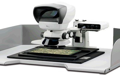
Manual visual inspection is performed by the experts working on the PCBA process. They can look for obvious defects in the PCB with their eyes i.e. Component placement after application of solder paste, contaminated solder paste, oxidation on the board, short circuit or aberration in the copper patterns and even missing components.

2. Automatic Optical Inspection (AOI)

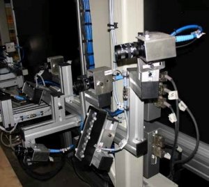
The standard technique of inspection of the PCB assembly is the automatic optical inspection which is done with the help of AOI machine. The AOI machine makes use of high resolution cameras to check the PCB for faults in design and assembly. It also checks for defects in the tracks and the soldering on the board. The AOI machine is fed with the design and drill files of the printed circuit board which than makes the comparison of the two designs and looks for aberrations. In case there are any differences, the AOI machine can pick it up and show the experts where there is any problem.
3. Structure Procedure Testing System (SPTS)

SPTS involves the image processing technique in order to detect any defect in the printed circuit board assembly. The SPTS technique does not require contact between the printed circuit board and the physical ground. The Structure Procedure Testing System (SPTS) is capable of providing repeatable quantitative measurement of the PCB.
4. X-Ray Inspection
The less common method of inspection is the x-ray inspection and used only for layered PCBs. The x-ray inspection allows seeing the inner layers of the PCBs and any problem which may be associated with them. A beam of x-ray is incident on the surface of the printed circuit board which passes through the PCB. The radiation causes the solder to radiate and an x-ray digital image is obtained which is in fact the density diagram of the solder paste. Analyzing this solder diagram, the durability of the solder can be analyzed.
5. X-Ray Layering System
An x-ray layering system is used in order to thoroughly analyze the multi-layer PCBA. It generates horizontal intersection by incident x-ray in such a manner or through spinning the PCB at an angle to the x-ray. This generates a layering image which can be very useful for analyzing the BGA and plated through hole. This analysis can significantly help improve the design process of the inner layers.

At Synergise PCB Inc. we apply all the standard testing methods in order to make our products stand out in the market. Our track record of producing highly reliable, long lasting and quality products is unmatchable in the printed circuit board market. Here we strive to take care of your special needs with our high standards of PCB designing and assemble.
