HDI or high density interconnect Printed Circuit Board is a way of developing high quality and complex circuit board devices in an efficient and cost effective manner. With the advancement in technology, there is need to accommodate more and more in small space. Devices are shrinking in size while their capability to do the functions and tasks they are designed far is increasing continuously. This has been made possible with the help of the high-density interconnected technology. The density of the connections, Vias, components, etc. in these circuit boards is much more as compared to the traditional circuit board.

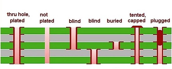
One of the most important specification of the HDI Printed Circuit Boards is that they have Vias demarked in smallest of proportions. Blind via and the Via in Pad technology and made the revolution of the HDI PCBs as they can allow the connection of different layers of the PCBs and the multilayer PCBs are better able to perform complex functions as compared to the traditional printed circuit boards. HDI technology and opened up new venues and developments in PCB Manufacturing.

A single layer of PCB with the help of the HDI technology can now support more and more components. This technology is behind all the advancement we have seen in smartphone industry where incredible features have been gathered in small and compact mobile sets.
Synergise PCB is one of the major HDI PCB manufacturer in Chicago, USA as we have the advanced capabilities of manufacturing good quality and effective HDI products. We have already delivered hundreds of large-scale projects for our clients all over the world. All the products are manufactured in USA under standard practices of manufacturing. This has helped us gain the trust of the customers and the experts in the field of HDI PCB and the industry in general.